HDI PCB---High density interconnects
Printed Circuited Boards
What is an HDI PCB?

-
4 layer rigid-flex PCB with HDI design
¥ 0.00Buy now
-
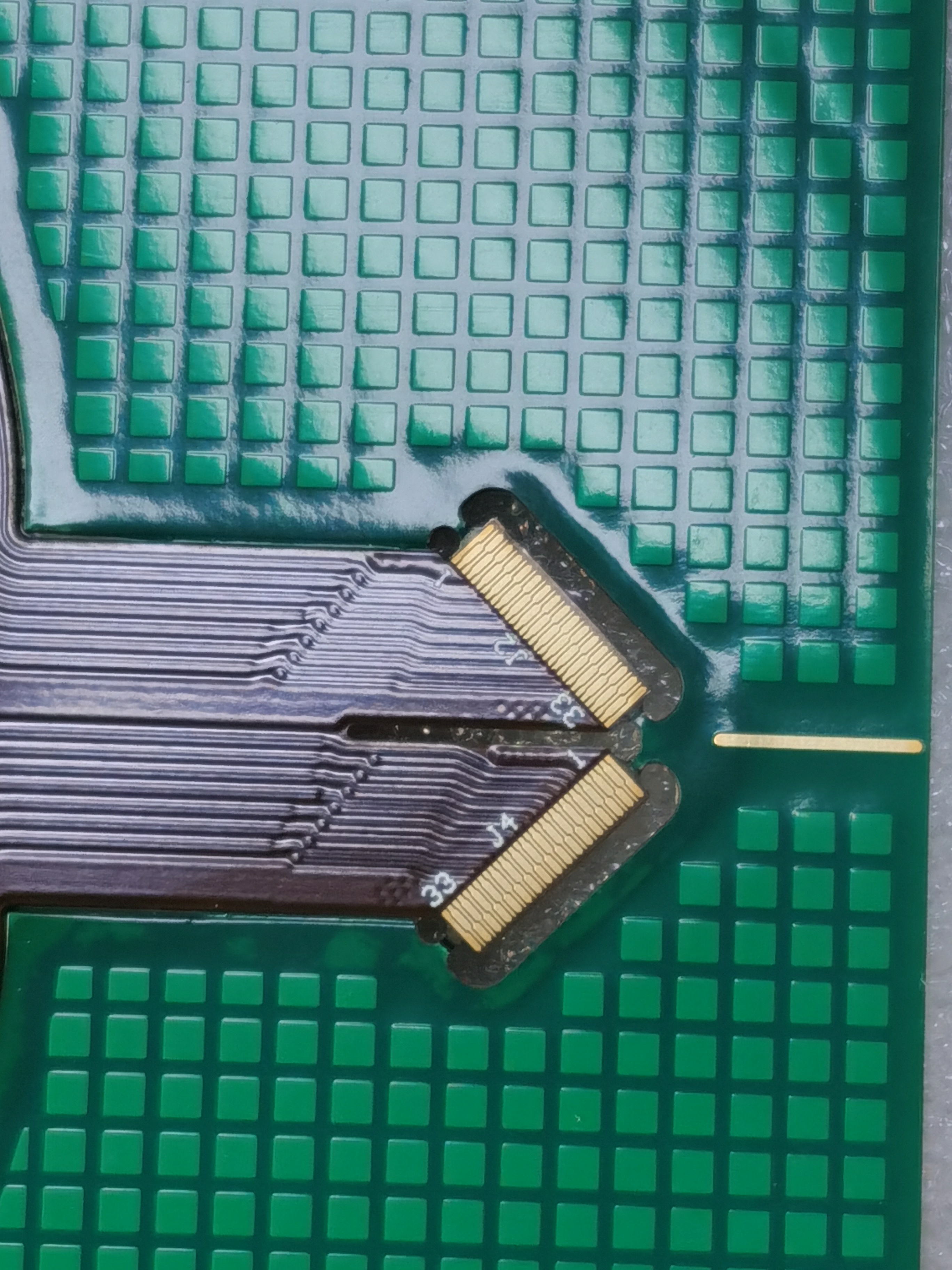
4 Layer HDI PCB with 0.38mm pitch BGA
4 Layer HDI PCB with 0.38mm pitch BGA
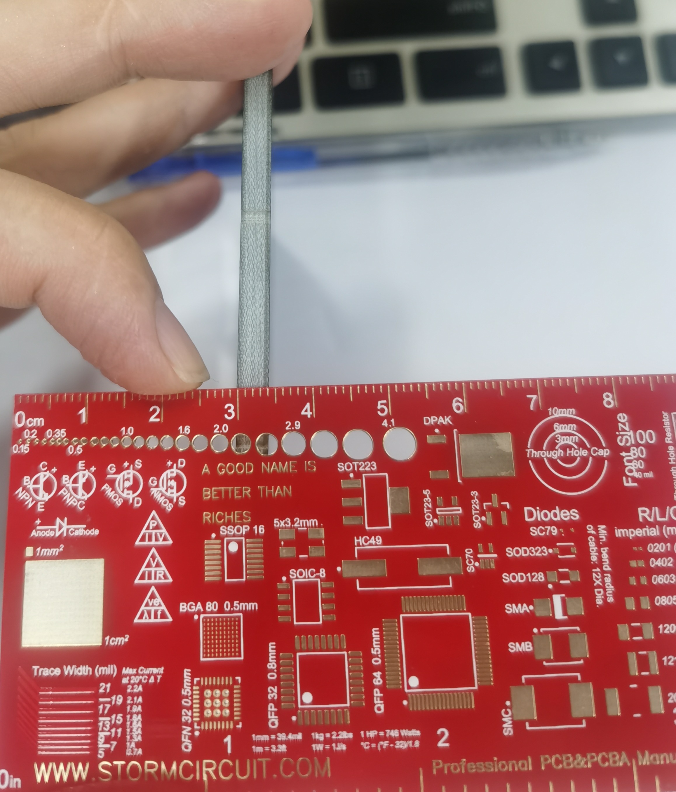
Min hole:0.15mm
Min trace/space: 0.076/0.0/76mm
0.38CSP
Blind Vias:L1-L2
Via in pad, POFV (Plated over filled vias)
4 layer 1.0mm Laser drilling¥ 0.00Buy now
-
Quick Turn HDI PCB--shipping in 5 days
Two designs,4 layer HDI PCB,0.4mm pitch BGA¥ 0.00Buy now
-
4 layer HDI with 0.4mm,shipping in 5 days.
4 layer HDI
HDI:L1-L2,L1-L3,
Via in pad
Half hole plating
Quick Turn shipping in 5 days.¥ 0.00Buy now
-
ENEPIG for RO4350B with blind vias from L1-L2,L3-L4
ENEPIG for RO4350B with blind vias from L1-L2,L3-L4¥ 0.00Buy now
-
4.4mm PCB with blind vias and countersink holes
4.4mm PCB ,4 Layer
Blind vias L1-L2 ,L3-L4
Countersink holes
Matt Black solder mask
Via in pad
12:1 (Thickness :min hole)¥ 0.00Buy now
-
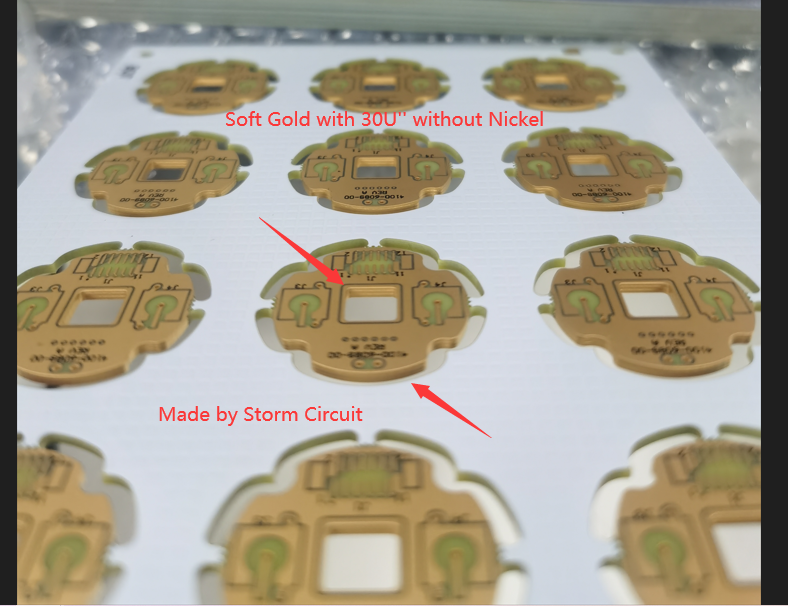
Soft Gold plating with 30 Micro inch PCB
FR4 :4 layer 1.6mm 1oz
Full gold at top and bottom side in units
Soft Gold with 30 micro inch
Edge plating
Black solder mask,white silkscreen¥ 0.00Buy now
-
0.4mm pitch BGA PCB with 0.1/0.1mm
0.4mm pitch BGA
BGA pad 0.2mm
4 layer 1.6mm
min trace/space 0.1/0.1mm¥ 0.00Buy now
-
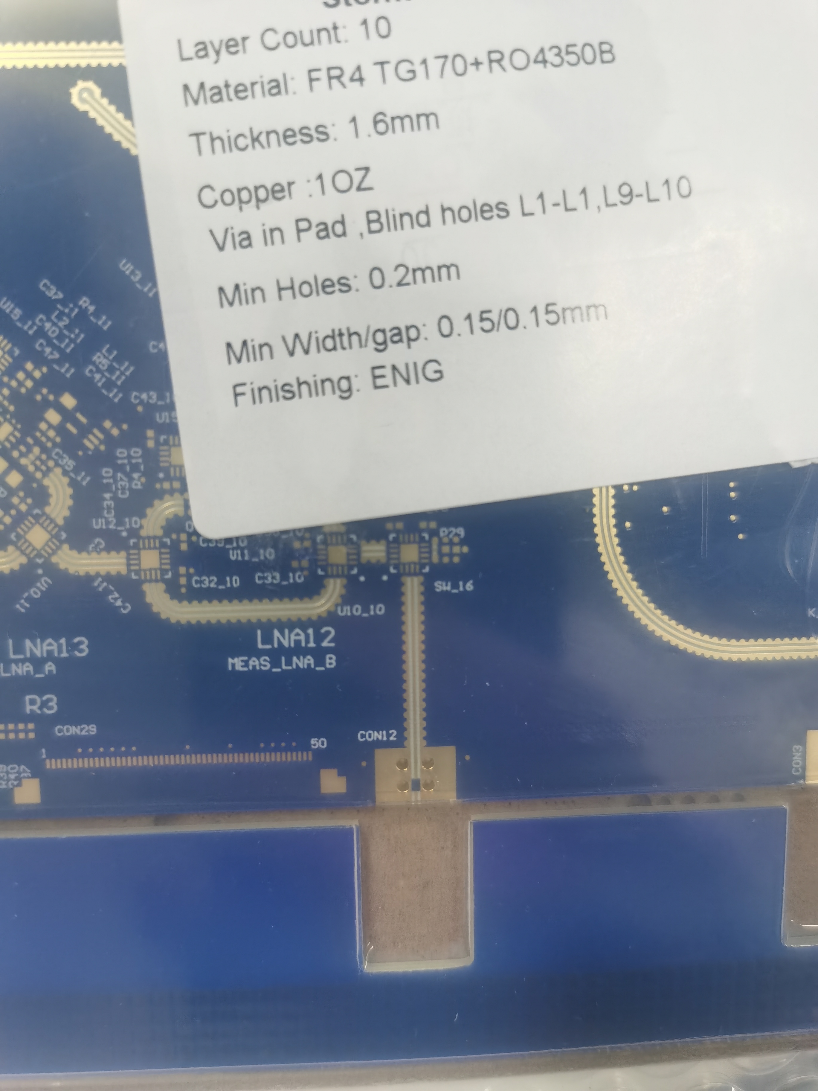
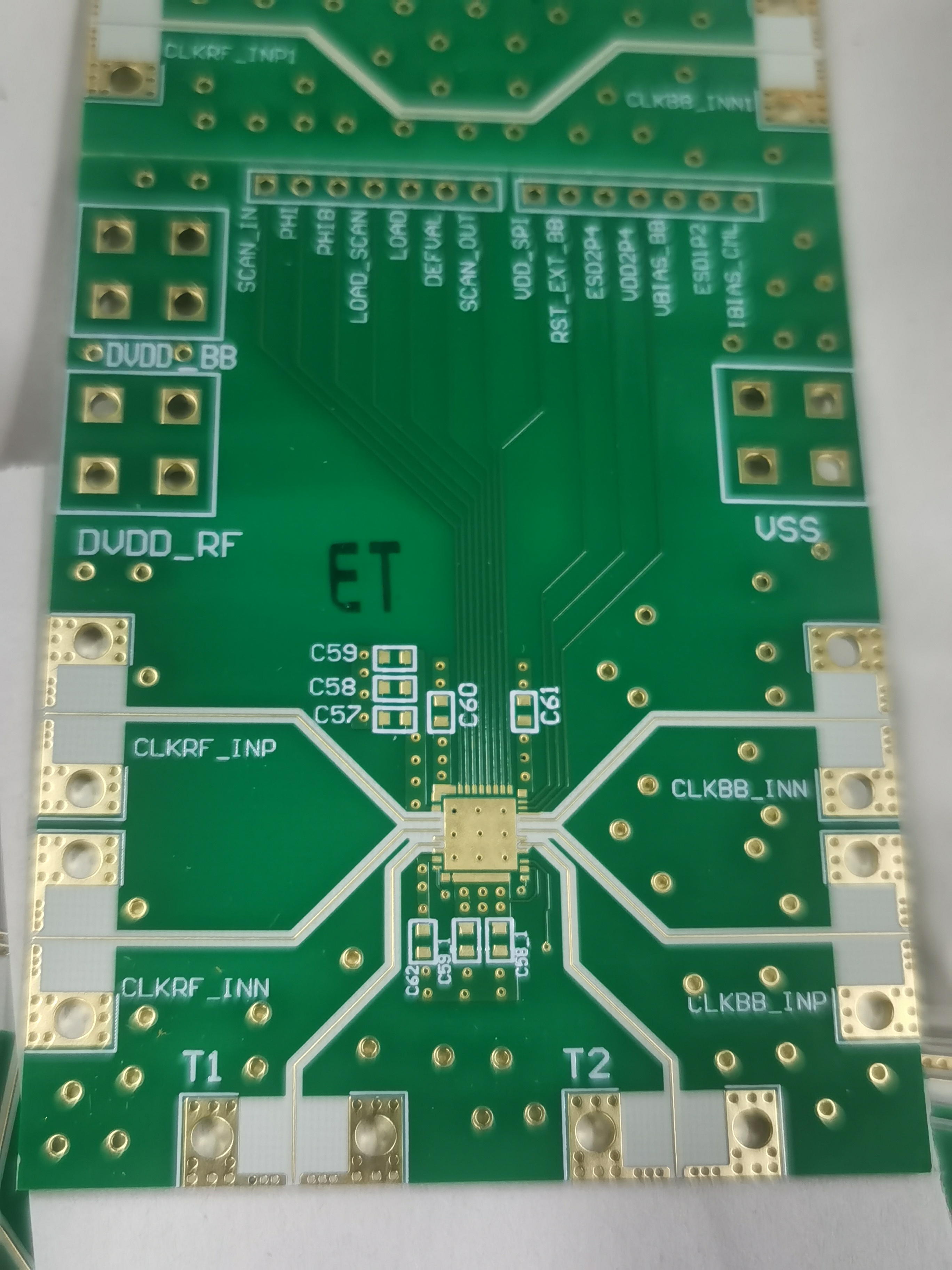
10 layer RF PCB with RO4350B+FR4
10 layer RF PCB with RO4350B+FR4
Blind vias L1-L2,L9-L10
Via in pad ,POFV
RO4350B 6.6mil¥ 0.00Buy now
-
L1-L2,L1-L3,L1-L6 8 layer HDI PCB
L1-L2,L1-L3,L1-L6
8 layer HDI PCB
Laser drilling
PCB material:TU-768, TG170
Via in pad¥ 0.00Buy now


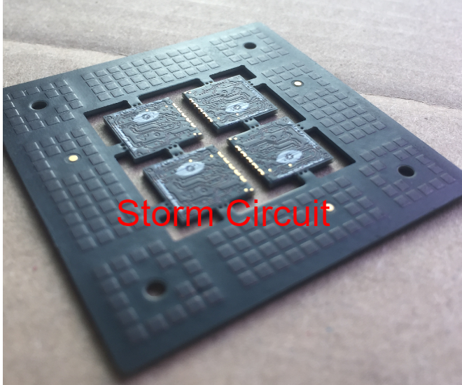
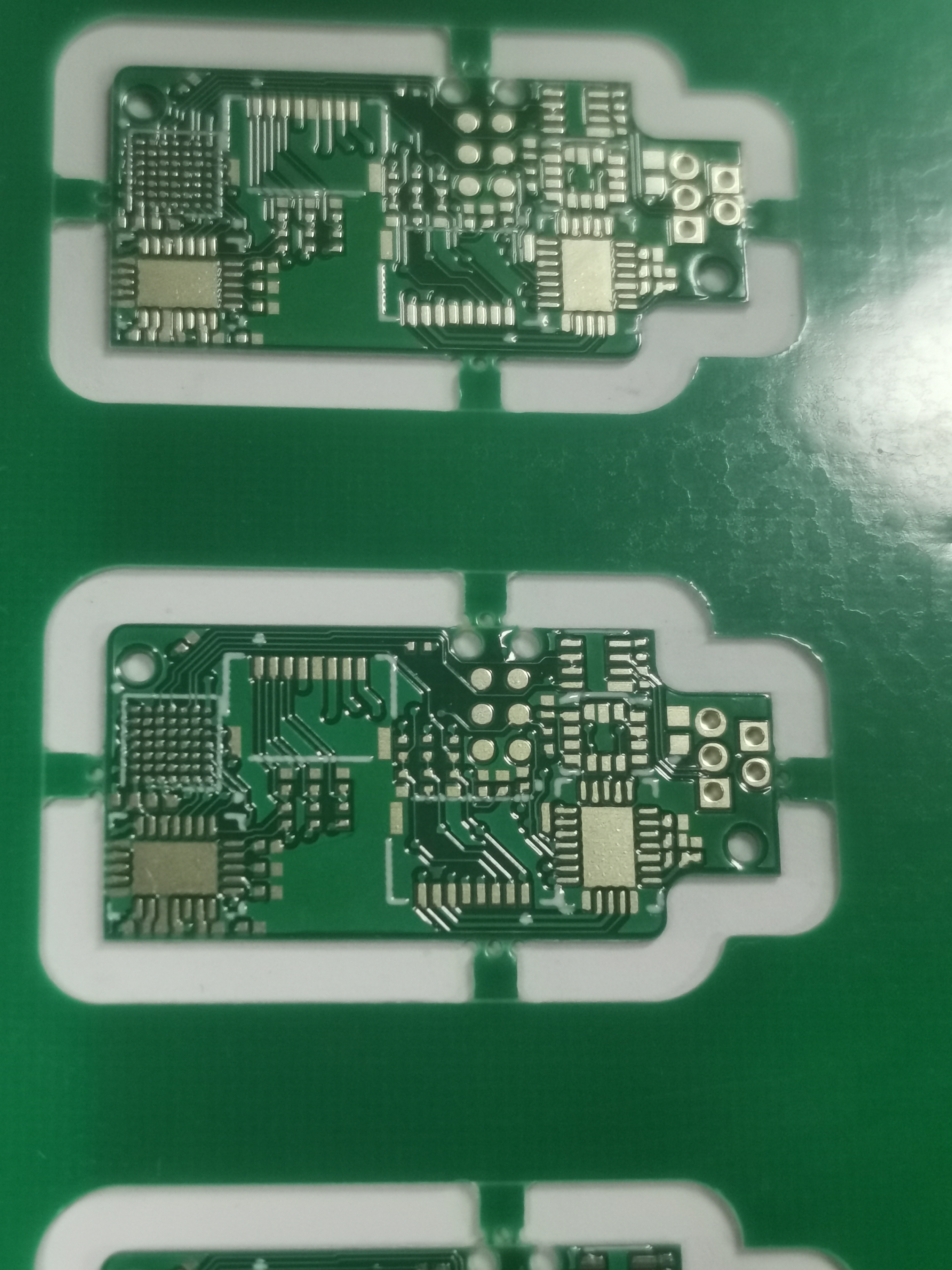
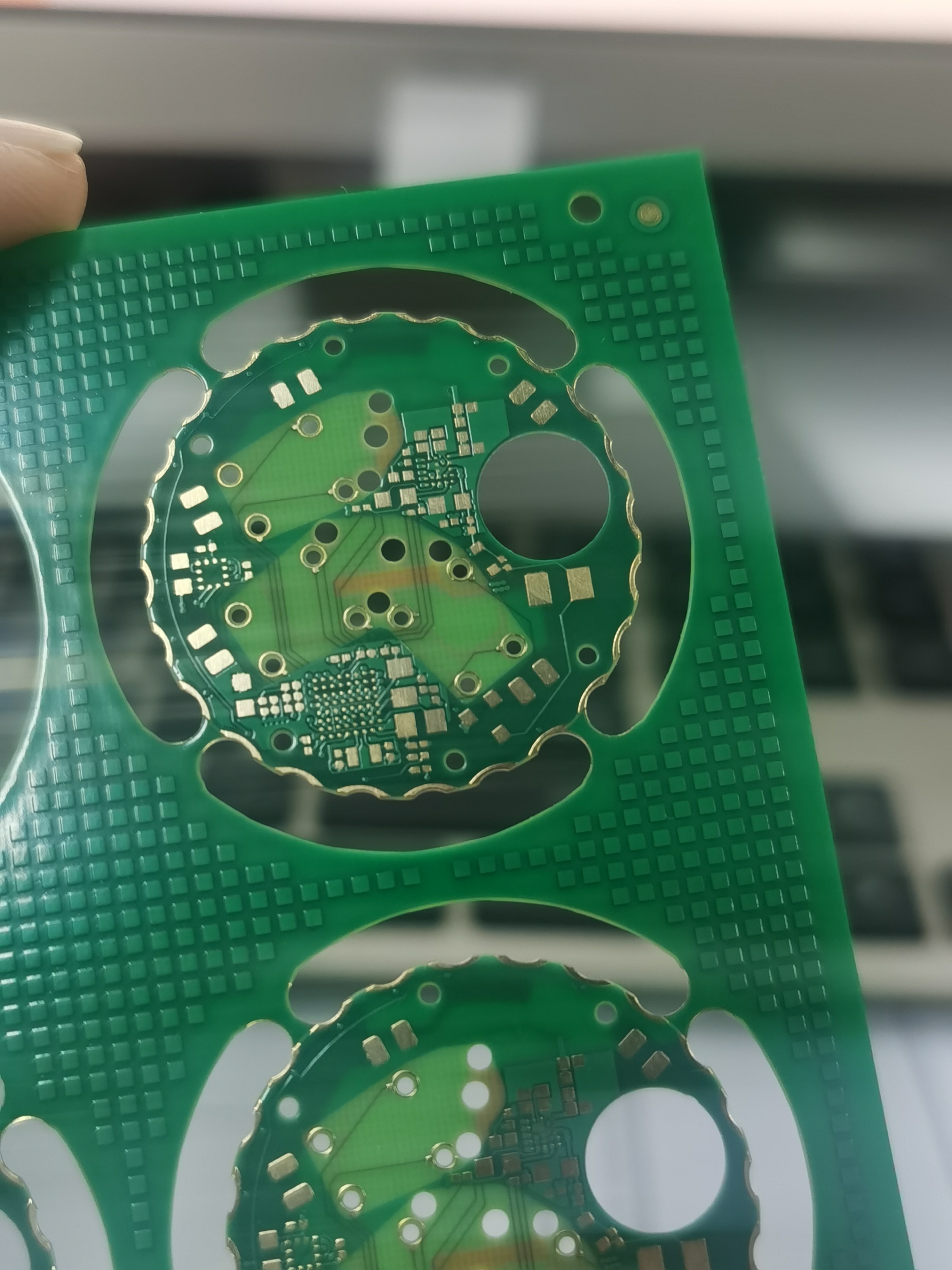
Our HDI PCB products
HDI PCBs capitalize on the latest technologies available to increase the functionality of PCBs using the same or less amount of area. This advancement in PCB technology is driven by the miniaturization of components and semiconductor packages that supports advanced features in revolutionary new products such as touch screen computing and 4G network communications,now it is 5G time,any layer technology is required for PCB .
HDI PCBs are characterized by high-density attributes including laser microvias, fine lines and high performance thin materials. This increased density enables more functions per unit area. Higher technology HDI PCBs have multiple layers of copper filled stacked microvias (Advanced HDI PCBs) which creates a structure that enables even more complex interconnections. These very complex structures provide the necessary routing solutions for today's large pin-count chips utilized in mobile devices and other high technology products. Most HDI boards are with burried/blind vias from 0.076-0..127mm.
Vias for HDI is 3-5 mil (0.076-0.127mm),line width is from 3-4mil(0.076-0.1mm). 0.8mm /0.5mm pitch BGA is usually for 1+N+1. Another thing is many customers did not know HDI board have to use special material--RCC (Resion Coated Copper),0.08mm thickness with copper.
0.4mm pitch BGA, means the space from BGA ball to another BGA ball is 0.4mm.
Many PCB designers do not know much how to design 0.4mm pitch BGA board,they make things very difficult to do .Here is a 0.4mm pitch BGA PCB design guide from TI OMAP processor. Pages 8 through 12 talk about pads, mask and vias. Obviously, you should consult similar materials written specifically for the part you are using, but Ti did a great job of covering all the issues here
Gerber file for 6 layer HDI board.
Specification:FR4,TG170,1.2mm,1oz for all layers.
min via:0.15mm, min trace/space:0.1/0.1mm.
Impedance control,
Black solder mask,ENIG
Blind/burried vias (L1-L2,L1-L3,L4-L6,L5-L6)


HDI example
- 2022-06-23
Storm Circuit Technology Ltd, Made in China with Love.
2009-2022