Printed Circuit Board Terminology
When customers talked with us ,we may have some misunderstandings.Especially for some new designers and students,they may not know much about Printed Circuit Boards,so here,we list some common words in the industry.Hope it helps some people who really want to know the PCB terminology.
* Annular Ring: This term refers to the copper pad area that is left after a hole is drilled through it. This ring is measured from the edge of the pad to the edge of the hole and is an important consideration in PCB design, as it allows an electrical connection to be made from one side of the hole to the other.
-
ꁸ Top
-
ꂅ 075528363585
-
ꀥ QR code

* AOI: Short for automated optical inspection, AOI refers to a type of inspection method used to find potential problems concerning soldering performance in multi-layer PCBs with components mounted on. The AOI equipment finds these issues by capturing images of the inner PCB surfaces, looking for any possible issues in terms of displacement, polarity etc.
*Aspect Ratio: Aspect ratio refers to the ratio between a PCB's thickness and diameter of its minimum via. It's best to keep aspect ratios low to improve plating quality and minimize potential via failures.that is if the min hole is 0.1mm, the board thickness can not be 1.6mm.
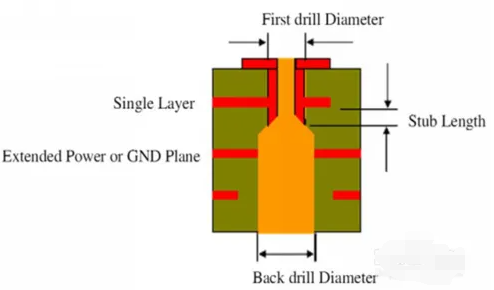
* Back Drilling: Primarily applied in multi-layer PCB fabrication, back-drilling helps improve signal integrity by removing stubs from plated through-holes. These stubs are unnecessary portions of via that extend into the hole, potentially causing reflections and other disturbances that damage signals.
* BGA: Short for ball grid array, this is a type of component packaging used in integrated circuits (ICs) for surface mounting. They can ensure high-speed efficiency since they use columns of balls instead of pins. BGAs are usually used to mount devices like microprocessors on PCBs permanently.
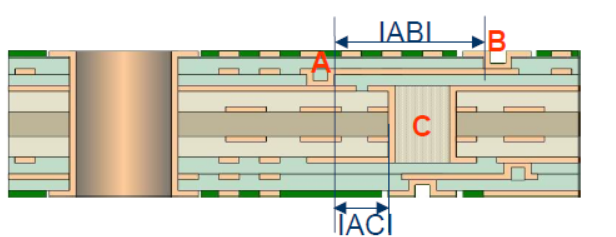
* Buried Via: This term is used to refer to a via connecting a top layer to one or more inner layers. In other words, a buried via can only be seen from one side of the board when looking at it from the outside.
* Blind Via:the via is from inner layer to another inner layer,that is we can not see the via from outside.
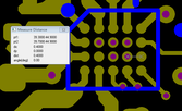
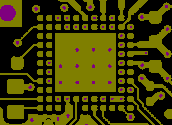
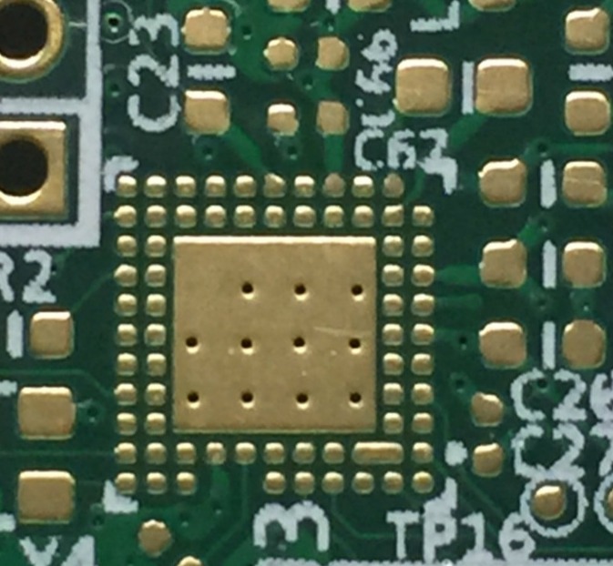
0.38mm pitch BGA,via in pad
* Ceramic Substrate Printed Board: This type of board is made with a ceramic substrate, to which other materials are bonded with alumina or aluminum nitride. The primary selling points for ceramic substrate boards are their excellent insulation capabilities, thermal conductivity, soft solderability and adhesive strength.
Panasonic Ceramic core PCB
* COB: Shorthand for chip-on-board, this term is a type of bare chip SMT technology. COB involves directly mounting integrated circuits to a PCB instead of packaging them first. Common in mass-produced gadgets and toys, COB can be identified by a black glob of plastic on a PCB, called a glob top. Underneath the glob, the chip connects to the board with fine wires.
* Copper Weight: This term is used to indicate thickness of copper foil on each layer of a PCB. It's typically expressed in ounces of copper per square foot.1OZ (0.035mmm)is standard weight,the max copper we made is 12OZ,that is thick copper PCB
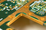
* Countersink Holes: These are cone-shaped holes that are drilled into a PCB. To allow a countersunk screw to sit flush with the PCB surface.Unlike the normal holes,the countersink hole has two dimensions,one side is bigger,another side is small.
16 Layer PCB with contersink holes
* Edge Plating: This is a term used for copper plating that stretches from the top to the bottom of a surface and along the edges of a board, allowing for edge soldering and connections.
* Gold Fingers: These are connectors found on the edge of a PCB after the board has been plated with gold. Hard, smooth and flat, these fingers are excellent conductors, supporting edge-to-edge connections. Gold fingers are usually hard gold with at least 5 micro inch.
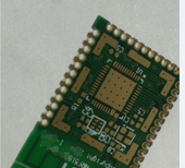
* Half-Cut/Castellated Holes: This refers to holes that are drilled on the edge of a board and plated, resulting in a half-circle hole on the edge of the PCB. This is common for PCBs designed for microchip testing.Also,we call it half hole plating. Castellated Holes are usually used in modules which will load on another main printed circuit board.
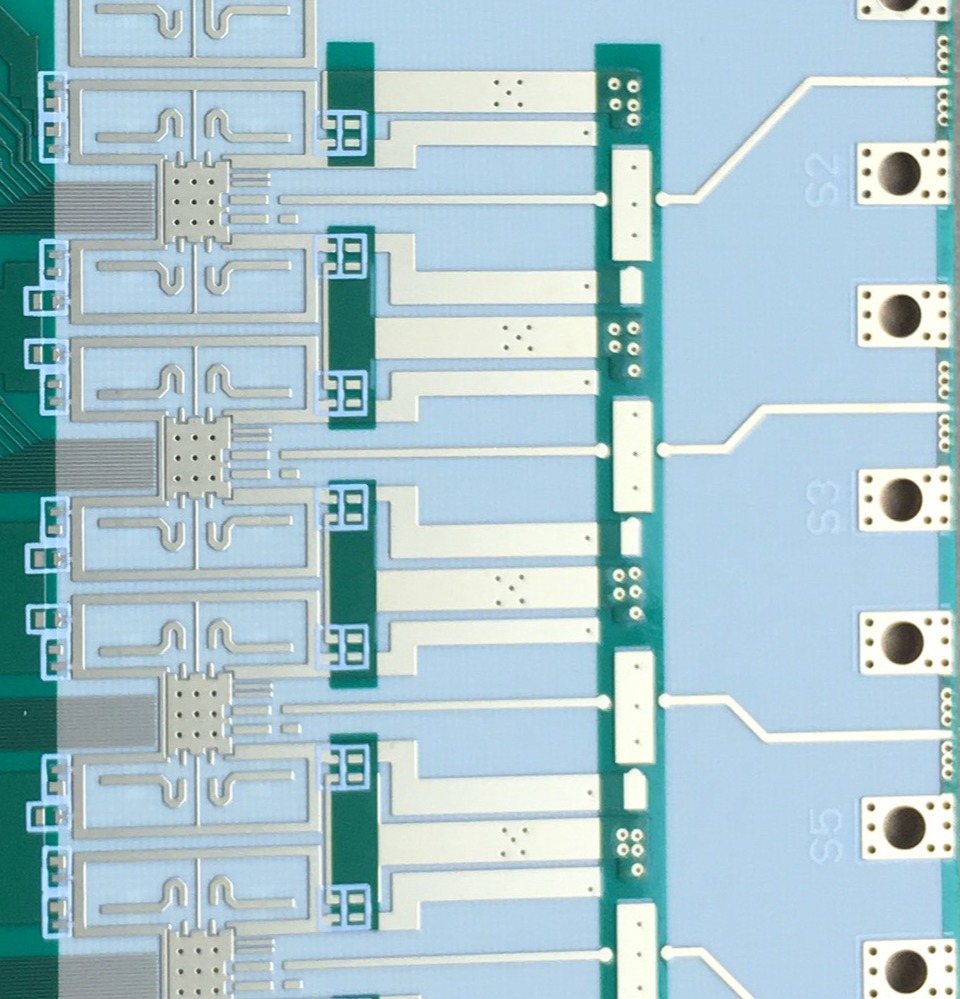
RF PCB: Short for radio frequency, RF is an electromagnetic frequency ranging between 300KHz and 300GHz. RF can also be a type of high-frequency electromagnetic signal. see our RF--high frequency PCB, RF PCB usually use high frequency material ,such as Roges material ,RO430B,RO4003C,RO5880,Taconic mateial , RF-35,TLF,etc. see our RF material .
RF PCB made by Storm Circuit
Tented Via: This is a type of via that has a dry film solder mask covering both its pad and its plated-thru hole. This solder mask insulates the via completely, protecting the PCB against shorts. Some vias are tented only on one side to allow for testing on the other.
Via: This term refers to plated through-holes that connect signals between traces on different layers of a PCB. These holes have conductive copper interiors to maintain an electrical connection.
Via Filled with solder mask/Via Plugged: This is a via that is filled with an epoxy resin. Once filled, copper can be soldered to the surface of the resin without influencing the final product.
Via in Pad: Also called a thru-hole on the pad, Plated over Filled Via (POFV),a via in pad functions as an electric connection between layers. It is useful for multi-layer components or for fixing the positions of components.Vin in pad are mostly at BGA area,there is no enough room to rout trace,so a hole at BGA pad to another layer is very helpful.
Via in pad in BGA area,gerber file
the vias on BGA pad filled and plated, we can not see holes from surface.
Regarding Flexible or Rigid-flex PCB terminology. please check here
Storm Circuit Technology Ltd, Made in China with Love.
2009-2022
