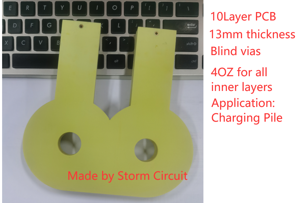
10 Layer PCB with 13mm ,4oz inner layers and blind vias
Our client in American University has a new PCB design for charging pile.Everyone knows the main problem in charging pile is the high voltage,normal PCB will be broken down by high voltage.
This PCB is very very thick, so far, this is the thickest we have made. it is about 13mm, 10 layer PCB and all inner layers are 4OZ, also,it has blind vias in inner layers.
The thickness is the key technology and the dielectric thickness too. The PCB requires dielectric thickness between L1/L2 and L9/L10 is 5mm, 5mm dielectric thickness can pass 20KV.
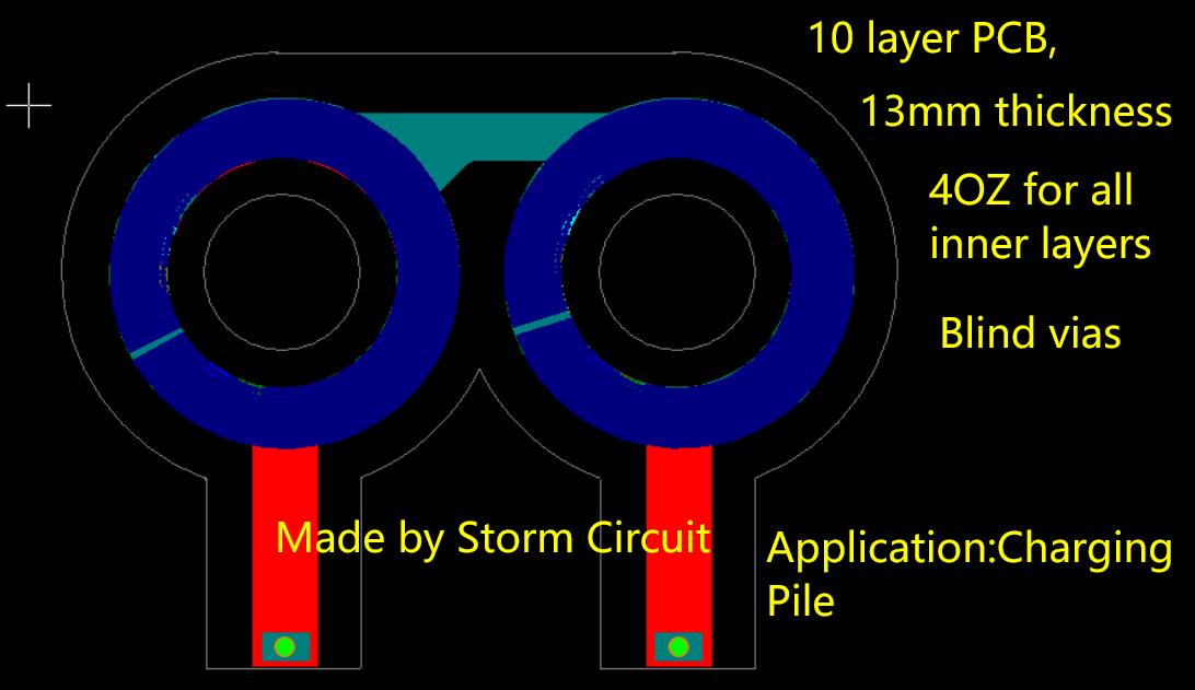 10 Layer Gerber file ,13mm Thickness, inner layers are 4OZ, Blind vais
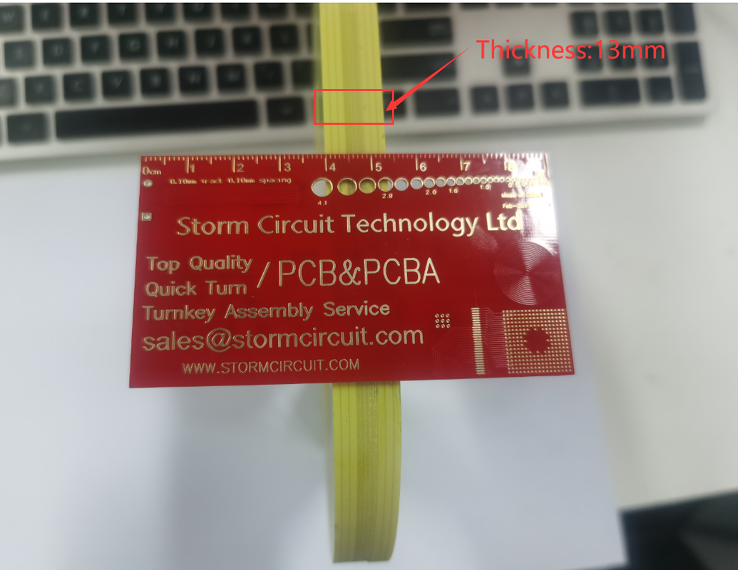
10 Layer thickness, 13mm
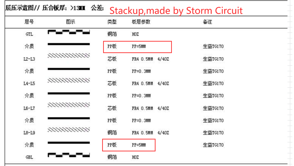
PCB stackup with 13mm for 10 layer
The key technology is the thickness, dielectric thickness is 5mm between L1/L2 and L9/L10.
So, the total thickness will be about 13mm,including 4OZ for all inner layers thickness.
If you are interested in such high layer with heavy copper,pls contact us .We are sure we can help you .