Do Not Layout like this
Many designers make very poor design files which will make PCB manufacturers make mistake .Poor design makes PCB fabrication very difficult. Here are some examples. Please do not layout like below.
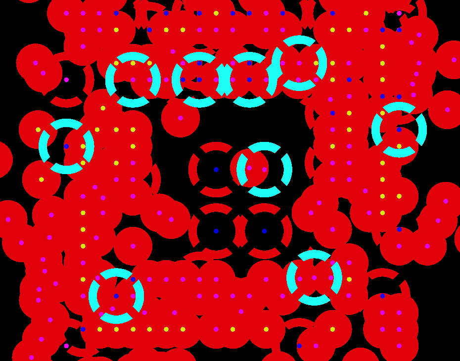
1) Do not make the isolated pads and theremal pads too big.
In inner layers, the too big isolated pads always make mistakes.TWe can pick up these issues in the HDI /high speed PCB under the BGA area. 0.2mm hole with 0.5mm isolated pad is very good.
See below, the highlighted are theremal pads, the customer wants the theremal holes connect to ground,but due to the too big isolated pads, connection was blocked. This design is a fail, PCB designer must reduce the theremal pads and isolated pads.
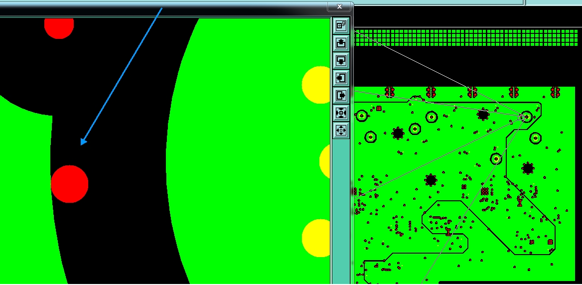
2, DO NOT MAKE CONNECTION TOO SMALL
Some customers made connection with a very small line,actually,that is a design issue. Our software did not pick up the issue.also,our Engineers did not too. That made the boards all failed. When boards testing ,we noted some boards passed but some failed. Our engineer checked carefully ,we zoomed up the view to max in the software and see 0.14mil connection. Thait is the root cause. who can pick up 0.14mil connection .
3,We will upate this article to avoid more design mistakes.