PCB Layout Recommendations for 0.4mm pitch BGA
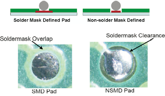
1,Pad Type
It is important to understand the pros, cons, and unknowns concerning the two most common types of
solder pads. Solder-Mask-Defined (SMD) and Non-Solder-Mask-Defined (NSMD) Pads
2,PCB Pad Dimensions for 0.4mm BGA Package
At the 0.4mm pitch, there is insufficient space between pads to allow a 3mil trace to run between pads
without incurring solder bridging. Therefore, except for the outside perimeter balls, all connections are
routed to the lower layers through VIP technology. With this technology, only six layers were needed for
the BeagleBoard.
For the BeagleBoard design, the desired finished pad size is equal to the solder ball diameter. Since no
traces run between the pads, the copper pad is enlarged to 280 mm (11mils). The solder mask opening is
set to 254 mm (10 mils).
With this arrangement, there is plenty of solder webbing between pads which helps prevent adjacent ball
solder bridging. For more information regarding additional parameters that impact the assembly of this
package.
Pad Type Solder Mask Defined
Pad Pitch A 400 mm (0.4mm)
Mask Opening B 254 mm (10mils)
Pad Size C 280 mm (11mils)
Mask Shape Round
Mask Web D 150 mm
Pad to Pad Clearance E 120 mm
Trace Allowed Between No
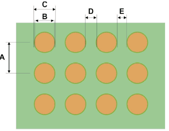
Recommendations for 0.4mm Pitch Packages - Top Layer
3,Etch Traps and Heat Sinks
The challenge with fine pitch board design is to insure that traces and vias don’t pull heat away from the
solder ball pad. This means that common sense routing circuit board guidelines are still useable. Also
beware of etch traps.

Small BGA pads don’t have much solder and depend on uniform heating for a good joint. Here are some
additional tips to insure that traces and vias don’t serve as heatsinks.
· Keep the trace smaller than the pad or via.
· Do not gang up pads with a copper pour such as around a ground plane.
· Use individual traces to interconnect the pads.
4,Vias and VIP (via in pad),or calls it with POFV (plated over filled vias)
One of the greatest benefits from package-on-package technology is the elimination of the complex,
expensive, and challenging task of routing high-speed memory lines from under the processor out to
memory. Instead, the memory sits on top of the processor and the connections are automatically made
during assembly.Except for the outer perimeter balls, routing for the BeagleBoard is done with VIP technology. Although
this was once a feared and expensive technology, recent studies and advances have eliminated nearly all
of the problems. In fact, VIP is becoming the dominate technology for high density boards and is providing
a cost effective alternative to conventional and offset vias.
The VIP methodology places the via directly under the device’s balls. However, this requires another step
to seal the via to prevent blowouts and voids. For the BeagleBoard, non-conductive, epoxy-filled vias were
used.
Please note, all blind/buried vias will be VIP (Via in pad). they will be filled with epoxy /resin and plated over filled vias, POFV.
After drilling, and depending on the board fabricator preferences, the BeagleBoard vias were filled with
non-conductive epoxy. It was used because it has a better match to the thermal expansion properties of
the board material.Once the vias are filled, cured, and planarized, they are then plated. This yields a flat copper plated cap
over the vias which facilitates component attachment. The VIP technology provides two primary benefits:
higher component density and improved routing.
 POFV--plated over filled vias., VIP--via in pad.
All vias must be capped or filled to prevent voids and out gassing. The images shows the effect of an uncapped via. The voids and damage occurs during reflow. The right picture is a failure caused by the excessive package movement during reflow, caused by out gassing.
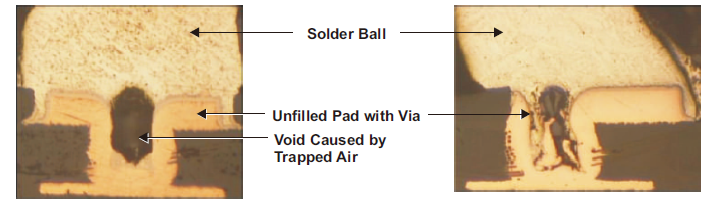
Effect af an Uncapped Via
It is strongly recommended that all vias be filled and/or capped, especially under BGA packages.