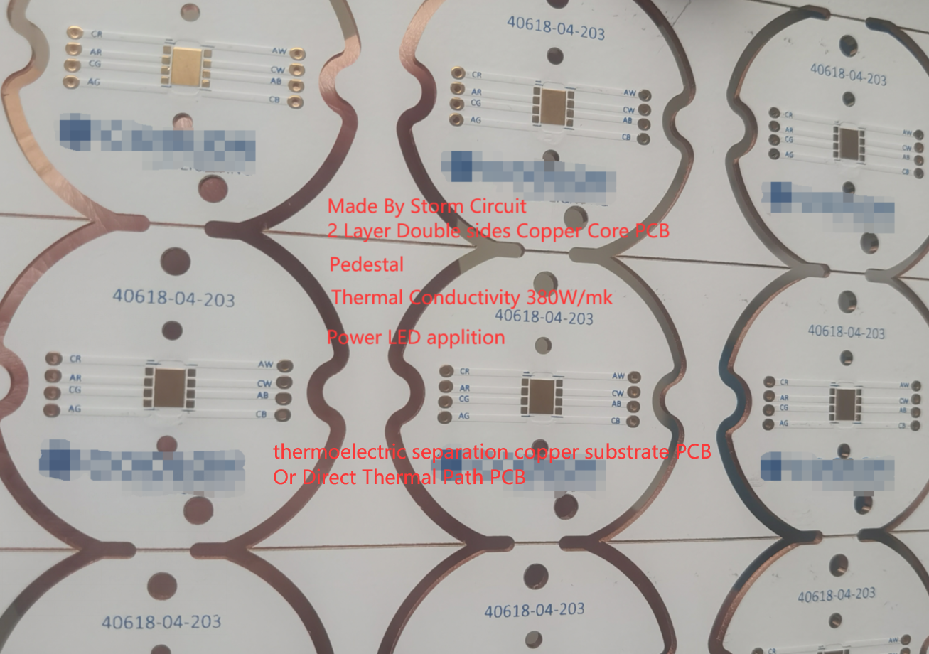
Thermoelectric separation copper substrate PCB---highest thermal conductivity with 380W/mk
ENIG
White solder mask, Blue silkscreen.
Thermoelectric separation copper substrate PCB---highest thermal conductivity with 380W/mk
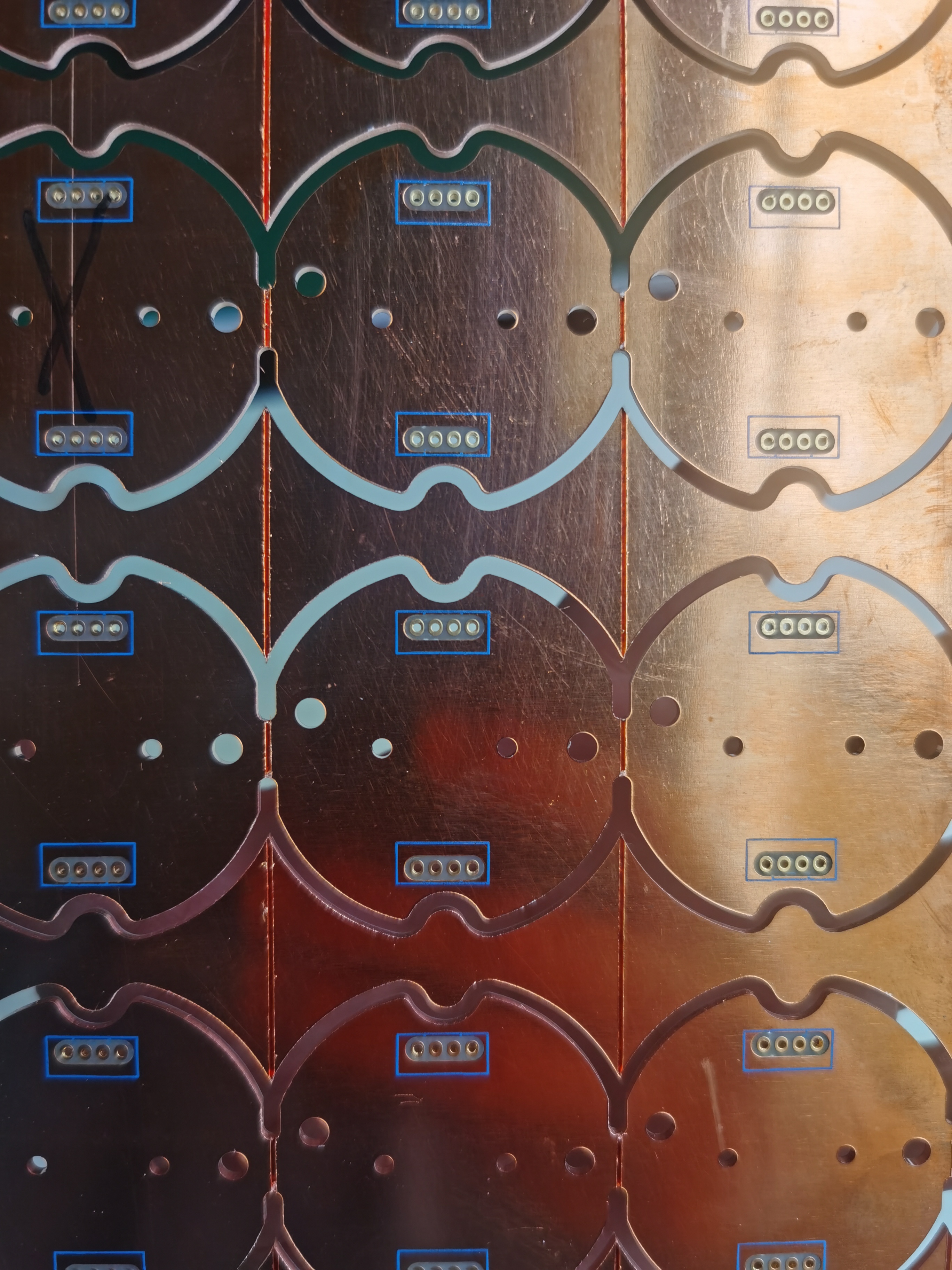
There are 8 plated holes at bottom side ,which customer will solder connectors from bottom side. And the important is the plated holes must be insulated from copper core.Also,the plated holes must be insulated from bottom copper.
So,we have to drill a bigger hole first, then fill with resin ,and plate to correct hole size.
The technology invented by Bergquist Company in the US and described in October 2010 OSRAM workshop (see attached document page 36),was originally called “Formed Pedestal”, which allowed base material to be formed planar to adjacent circuitry copper layers for connection to an isolated thermal pad of high power LED. While the process of creating the “Formed Pedestal” now is not made using punch tools, the name “Pedestal” does reflect the physical build-up of the PCB.
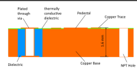
Plated through via (in our case plated through pads for T/H component) are insulated from the base copper material.
In China, we usually call this technology as Thermoelectric separation copper substate PCB or Direct Thermal PCB (DTP)
“Pedestal” for connection to an isolated thermal pad of the LED (large pad in the middle of LED footprint) is a part of the base,and has no dielectric on it, and mounting holes are just drilled holes, going through dielectric layer on top and the copper base. They are to secure PCB within the enclosure and provide reliable thermal contact between the PCB and enclosure, acting as a heat sink.
The exact cross-section of the pedestal is shown on page 41 of the document, and as the inventors of technology use the word “Pedestal”,
The thermal conductivity for Normal Aluminum Core PCB is only 1-8W/mk,however,this technology --Direct Thermal PCB has highest thermal conductivity ---380W/mk.
